Qubits and Nanosensors in a 2D Material
New research pins quantum technological hopes on a graphenelike semiconducting material
A new study has discovered rarified quantum properties in an everyday material that could yield a new approach to quantum computers and extremely sensitive measuring devices.
In one sense, the research represents only a small step forward, because these quantum properties are already well studied and understood in other materials and experimental setups. But in another, it may be an important departure point because discovering ways to manipulate such submicroscopic phenomena in cheap, accessible, everyday materials would solve the paradox of quantum technologies today.
The paradox goes something like this: If quantum states—such as an individual electron’s spin—an be easily manipulated and lashed to other individual electron spins, they open up a cornucopia of applications including quantum computers, microscopic atomic clocks, GPS units, and extremely fine measuring devices such as nanoscale microscopes, hypersensitive accelerometers, and divining rods capable of detecting gas deposits, biomolecules, and weapons of mass destruction.
But as of this point, tapping such tiny technological potential typically requires gigantic, clumsy laboratory devices like vacuum chambers, cryogenic coolers, and laser atom traps. Which is why discovering the right host material would be so significant. Tiny quantum technologies in a tiny device or microchip would be revolutionary.
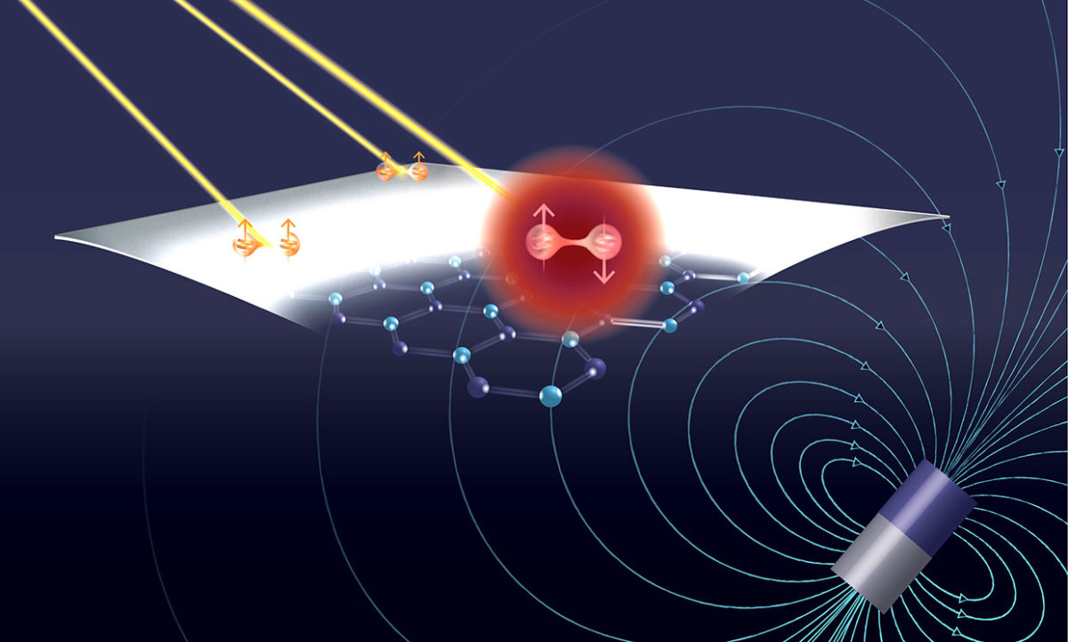
The new research, published in the 15 January issue of Nature Communications, concerns extremely thin layers of a 2D material laid out in a hexagonal grid much like the carbon supermaterial graphene. But, unlike electrically conductive graphene, this material, called hexagonal boron nitride (h-BN), is a semiconductor.
As with semiconductor breakthroughs of the 1940s and ’50s that enabled the computer revolution from which we have derived myriad benefits, the h-BN discovery harnesses defects in the material’s lattice. Certain defects—though the researchers have yet to discover which—appear to shield individual electron spins deep within the semiconductor’s wide bandgap.
“Quantum information science and quantum engineering is a constant battle between isolation and control,” says Lee Bassett, assistant professor of electrical and systems engineering at the University of Pennsylvania. “We need things to be isolated so they are not randomly talking to everything in their environment. But we need them to talk to their environment because we need to control them.”
Bassett says some quantum technologies have already sprung up around an analogous 3D material—diamond that contains nitrogen defects sprinkled through its carbon lattice. Diamonds with so-called nitrogen vacancies (NV) have been studied since the late 1990s. Researchers have since discovered these NV diamond defects could shelter long-lived individual electron spins. Bassett says there are today several companies pursuing quantum technologies using NV centers in diamond.
Yet, NV in diamond is a 3D material. So controlling individual states, let alone dozens or hundreds entangled together, is very challenging. [READ MORE]