
IBM Introduces the World’s First 2-nm Node Chip
New chip milestone offers greater efficiency and performance
IBM has become the first in the world to introduce a 2-nanometer (nm) node chip. IBM claims this new chip will improve performance by 45 percent using the same amount of power, or use 75 percent less energy while maintaining the same performance level, as today’s 7 nm-based chips. To give some sense of scale, with 2-nm technology, IBM could put 50 billion transistors onto a chip the size of a fingernail.
The foundation of the chip is nanosheet technology in which each transistor is made up of three stacked horizontal sheets of silicon, each only a few nanometers thick and completely surrounded by a gate. Nanosheet technology is poised to replace so-called FinFet technology named for the fin-like ridges of current-carrying silicon that project from the chip’s surface. The life expectancy of FinFet has been more or less set at the 7-nm node. If it were to go any smaller, transistors would become difficult to switch off: Electrons would leak out, even with the three-sided gates.
One can’t help but sense a bit of one-upmanship in IBM’s development after Taiwan Semiconductor Manufacturing Co. (TSMC) decided to stay with FinFETs for its next generation process, the 3-nanometer node. While IBM’s manufacturing partner, Samsung, does plan to use nanosheet technology for its 3-nm node chips, IBM outdid them both by using nanosheets and going down another step to a 2-nm node.
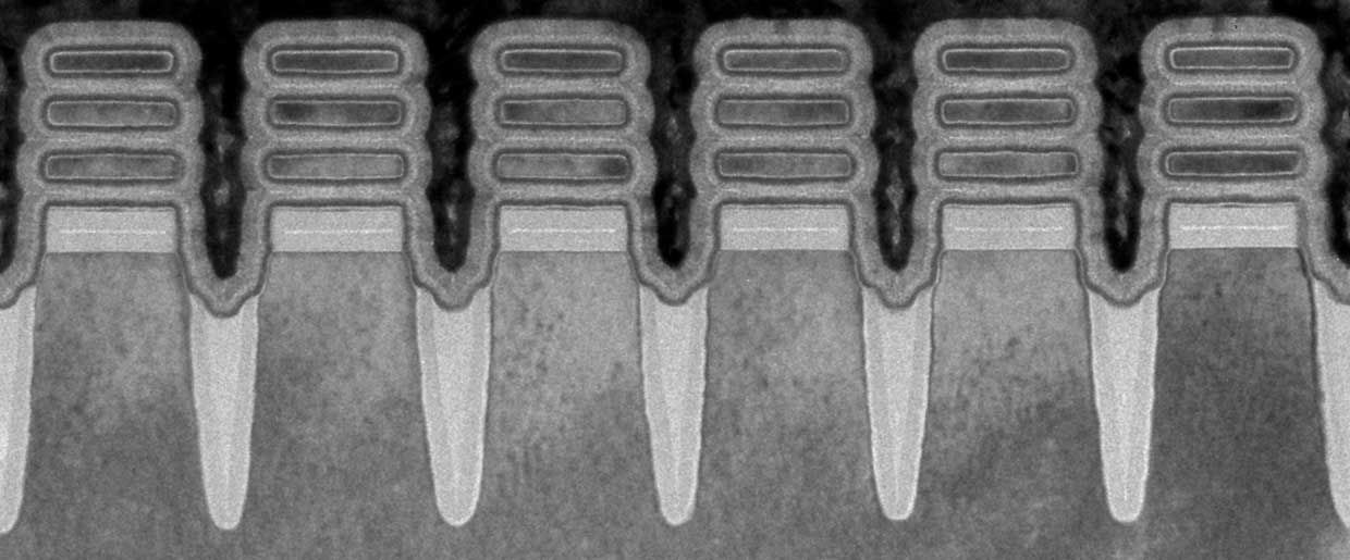
To further enable the chip beyond nanosheets, IBM has used bottom dielectric isolation (BDI) to produce 12-nm gate lengths, a feature representing a first in the industry. BDI involves the introduction of a dielectric layer underneath both the source and drain gate regions. The benefits of implementing a full BDI scheme is to reduce sub-channel leakage, immunity to process variation and power-performance improvement.
Another first for these chips was IBM’s application of extreme-ultraviolet lithography (EUV) patterning to the front-end-of-line (FEOL) where the individual devices (transistors, capacitors, resistors, etc.) are patterned in the semiconductor. After a decade of hand-wringing over whether EUV would ever deliver on its promises, it has in the last few years become a keystone for enabling 7-nm chips. Now, in this latest step in its evolution, EUV patterning has made it possible for IBM to produce variable nanosheet widths from 15 nm to 70 nm.
IBM has also developed a multi-threshold-voltage (Multi-VT) scheme for both system-on-a-chip (SoC) and high-performance computing (HPC) applications. Threshold voltages—also known as gate voltages—are the minimum voltage differential needed between a gate and the source to create a conducting path between the source and drain terminals. Multi-VT schemes leverage gates with different thresholds to optimize for power, timing, and area constraints. [READ MORE]
Comments :