
Behind Intel’s HPC Chip that Will Pierce the Exascale Barrier
On Monday, Intel unveiled new details of the processor that will power the Aurora supercomputer, which is designed to become one of the first U.S.-based high-performance computers (HPCs) to pierce the exaflop barrier—a billion billion high-precision floating-point calculations per second. Intel Fellow Wilfred Gomes told engineers virtually attending the IEEE International Solid State Circuits Conference this week that the processor pushed Intel’s 2D and 3D chiplet integration technologies to the limits.
The processor, called Ponte Vecchio, is a package that combines multiple compute, cache, networking, and memory silicon tiles, or “chiplets.” Each of the tiles in the package is made using different process technologies, in a stark example of a trend called heterogeneous integration.
Ponte Vecchio is, among other things, a master class in 3D integration.
The result is that Intel packed 3,100 square millimeters of silicon—nearly equal to four Nvidia A100 GPUs—into a 2,330 mm2 footprint. That’s more than 100 billion transistors across 47 pieces of silicon.
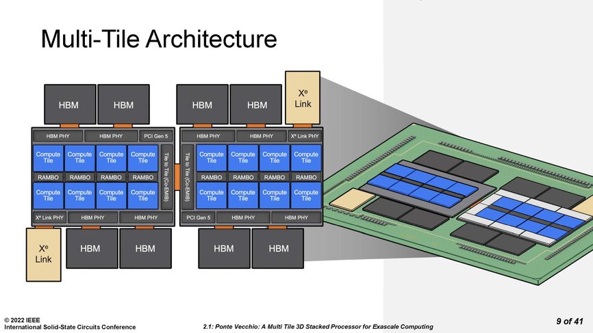
Ponte Vecchio is made of multiple compute, cache, I/O, and memory tiles connected using 3D and 2D technology.Source: Intel Corp.
Ponte Vecchio is, among other things, a master class in 3D integration. Each Ponte Vecchio processor is really two mirror image sets of chiplets tied together using Intel’s 2D integration technology Co-EMIB. Co-EMIB forms a bridge of high-density interconnects between two 3D stacks of chiplets. The bridge itself is a small piece of silicon embedded in a package’s organic substrate. The interconnect lines on silicon can be made narrower than on the organic substrate. Ponte Vecchio’s ordinary connections to the package substrate were 100 micrometers apart, whereas they were nearly twice as dense in the Co-EMIB chip. Co-EMIB dies also connect high-bandwidth memory (HBM) and the Xe Link I/O chiplet to the “base silicon,” the largest chiplet, upon which others are stacked.
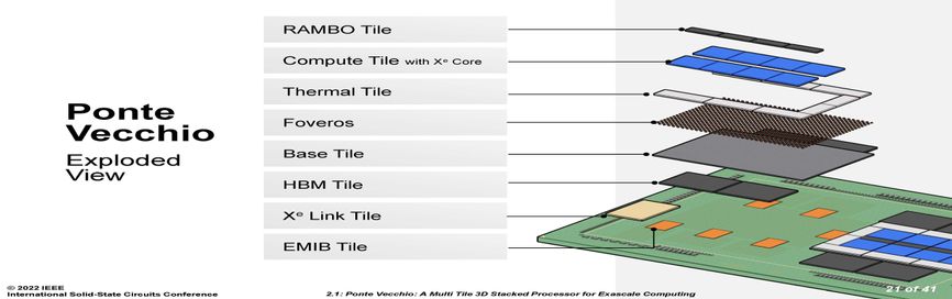
The parts of Ponte Vecchio.Source: Intel Corp.
Each set of eight compute tiles, four SRAM cache chiplets called RAMBO tiles, and eight blank “thermal” tiles meant to remove heat from the processor is connected vertically to a base tile. This base provides cache memory and a network that allows any compute tile to access any memory.
Notably, these tiles are made using different manufacturing technologies, according to what suited their performance requirements and yield. The latter term, the fraction of usable chips per wafer, is particularly important in a chiplet integration like Ponte Vecchio, because attaching bad tiles to good ones means you’ve ruined a lot of expensive silicon. The compute tiles needed top performance, so they were made using TSMC’s N5 (often called a 5-nanometer) process. The RAMBO tile and the base tile both used Intel 7 (often called a 7-nanometer) process. HBM, a 3D stack of DRAM, uses a completely different process than the logic technology of the other chiplets, and the Xe Link tile was made using TSMC’s N7 process. [READ MORE]