
Single-Chip Processors Have Reached Their Limits
Apple once again surprised enthusiasts and analysts with its announcement of the M1 Ultra, a variant of the M1 Max that effectively fuses two chips into one. The result is a dual-chip design viewed by software as a single piece of silicon. Nvidia delivered similar news at the GPU Technology Conference 2022, where CEO Jensen Huang announced that the company will fuse two of the company’s new Grace CPU processors into a single “Superchip.”
These announcements target different markets. Apple has its sights set on the consumer and professional workstation world, while Nvidia intends to compete in high-performance computing. Yet the divergence in purpose only underscores the broad challenges rapidly bringing the era of monolithic chip design to an end.
Multichip design isn’t new, but the idea has surged in popularity in the last five years. AMD, Apple, Intel, and Nvidia have all dabbled to varying degrees. AMD has pursued chiplet design with its EPYC and RYZEN processors. Intel plans to follow suit with Sapphire Rapids, an upcoming architecture for the server market built on the use of chiplets it calls “tiles.” Now Apple and Nvidia have joined the party—though with designs that target significantly different markets.
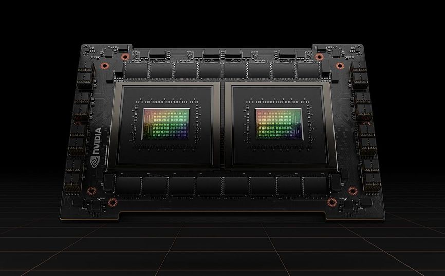
Nvidia’s Grace CPU SuperchipNvidia
The shift toward multichip design is driven by the challenge of modern chip manufacturing. Miniaturization of transistors has slowed, yet growth in transistor counts in leading-edge designs shows no sign of slowing.
Apple’s M1 Ultra has 114 billion transistors and a die area (or fabrication area) of roughly 860 square millimeters (an official figure for the M1 Ultra is unavailable, but a single M1 Max chip has a die area of 432 mm2). The transistor count of Nvidia’s Grace CPU is still under wraps, but the Hopper H100 GPU announced alongside the Grace CPU includes 80 billion transistors. For perspective, AMD’s 64-core EYPC Rome processor, released in 2019, has 39.5 billion transistors.
Transistor counts this high push modern chip production to its extremes, making multichip design more attractive. “Multichip module packaging has enabled the chip players to give better power efficiency and performance [with regard] to monolithic designs, as the die size for chips becomes larger and wafer-yield issues become more prominent,” Akshara Bassi, a research analyst at Counterpoint Research, said in an email. Aside from Cerebras, a startup attempting to build chips that span the entirety of a silicon wafer, the chip industry seems in agreement that monolithic design is becoming more trouble than it’s worth.
This shift towards chiplets has occurred in step with support from manufacturers. Taiwan Semiconductor Manufacturing Co. is a leader, offering a suite of advanced packaging called 3DFabric. Technologies that fall under the umbrella of 3DFabric are used by AMD in some EPYC and RYZEN processor designs and are almost certainly used by Apple for M1 Ultra (Apple has not confirmed this, but the M1 Ultra is produced by TSMC). Intel has its own packaging technologies, such as EMIB and Foveros. Though originally meant for Intel’s own use, the company’s chip-manufacturing technology is becoming relevant to the broader industry as Intel Foundry Services opens its doors. [READ MORE]