
3D-Stacked CMOS Takes Moore’s Law to New Heights
Perhaps the most far-reaching technological achievement over the last 50 years has been the steady march toward ever smaller transistors, fitting them more tightly together, and reducing their power consumption. And yet, ever since the two of us started our careers at Intel more than 20 years ago, we’ve been hearing the alarms that the descent into the infinitesimal was about to end. Yet year after year, brilliant new innovations continue to propel the semiconductor industry further.
Along this journey, we engineers had to change the transistor’s architecture as we continued to scale down area and power consumption while boosting performance. The “planar” transistor designs that took us through the last half of the 20th century gave way to 3D fin-shaped devices by the first half of the 2010s. Now, these too have an end date in sight, with a new gate-all-around (GAA) structure rolling into production soon. But we have to look even further ahead because our ability to scale down even this new transistor architecture, which we call RibbonFET, has its limits.
So where will we turn for future scaling? We will continue to look to the third dimension. We’ve created experimental devices that stack atop each other, delivering logic that is 30 to 50 percent smaller. Crucially, the top and bottom devices are of the two complementary types, NMOS and PMOS, that are the foundation of all the logic circuits of the last several decades. We believe this 3D-stacked complementary metal-oxide semiconductor (CMOS), or CFET (complementary field-effect transistor), will be the key to extending Moore’s Law into the next decade.
The Evolution of the Transistor
Continuous innovation is an essential underpinning of Moore’s Law, but each improvement comes with trade-offs. To understand these trade-offs and how they’re leading us inevitably toward 3D-stacked CMOS, you need a bit of background on transistor operation.
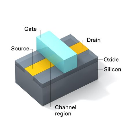
Every metal-oxide-semiconductor field-effect transistor, or MOSFET, has the same set of basic parts: the gate stack, the channel region, the source, and the drain. The source and drain are chemically doped to make them both either rich in mobile electrons ( n-type) or deficient in them (p-type). The channel region has the opposite doping to the source and drain.
In the planar version in use in advanced microprocessors up to 2011, the MOSFET’s gate stack is situated just above the channel region and is designed to project an electric field into the channel region. Applying a large enough voltage to the gate (relative to the source) creates a layer of mobile charge carriers in the channel region that allows current to flow between the source and drain.
As we scaled down the classic planar transistors, what device physicists call short-channel effects took center stage. Basically, the distance between the source and drain became so small that current would leak across the channel when it wasn’t supposed to, because the gate electrode struggled to deplete the channel of charge carriers. To address this, the industry moved to an entirely different transistor architecture called a FinFET. It wrapped the gate around the channel on three sides to provide better electrostatic control.
Transistor Evolution
Intel introduced its FinFETs in 2011, at the 22-nanometer node, with the third-generation Core processor, and the device architecture has been the workhorse of Moore’s Law ever since. With FinFETs, we could operate at a lower voltage and still have less leakage, reducing power consumption by some 50 percent at the same performance level as the previous-generation planar architecture. FinFETs also switched faster, boosting performance by 37 percent. And because conduction occurs on both vertical sides of the “fin,” the device can drive more current through a given area of silicon than can a planar device, which only conducts along one surface.
However, we did lose something in moving to FinFETs. In planar devices, the width of a transistor was defined by lithography, and therefore it is a highly flexible parameter. But in FinFETs, the transistor width comes in the form of discrete increments—adding one fin at a time–a characteristic often referred to as fin quantization. As flexible as the FinFET may be, fin quantization remains a significant design constraint. The design rules around it and the desire to add more fins to boost performance increase the overall area of logic cells and complicate the stack of interconnects that turn individual transistors into complete logic circuits. It also increases the transistor’s capacitance, thereby sapping some of its switching speed. So, while the FinFET has served us well as the industry’s workhorse, a new, more refined approach is needed. And it’s that approach that led us to the 3D transistors we’re introducing soon. [READ MORE]